


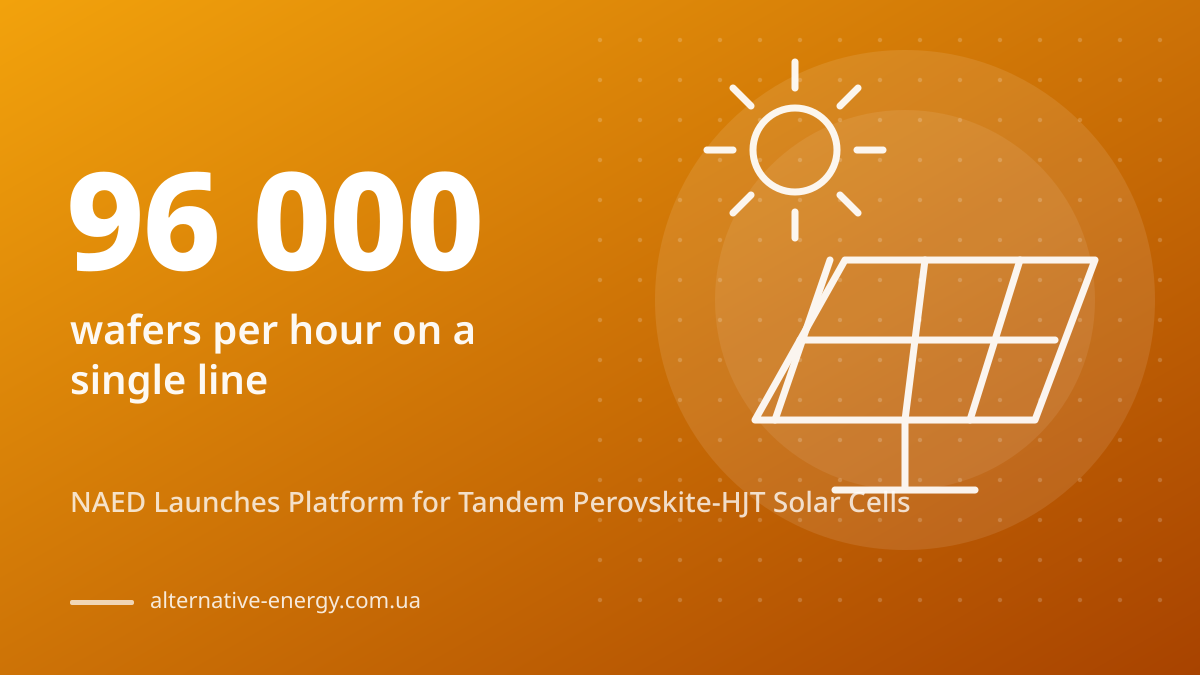
Miami-based NAED Energy has unveiled the PV-1 PECVD-V — a vertical in-line deposition platform designed for high-volume manufacturing of tandem perovskite-HJT solar cells. According to pv-tech.org, the system’s rated throughput reaches 96,000 wafers per hour, while its T2X tandem cells target a conversion efficiency of 30%. The equipment is manufactured entirely in the United States using the company’s aerospace-grade CNC production facilities.
At a glance:
- Throughput — 96,000 wafers per hour (twice that of NAED’s previous platform).
- Target efficiency of two-terminal T2X tandem cells — 30%.
- T2X glass-glass modules start at 600 W.
- PV-1 PECVD-V integrates PECVD and PVD processes on a single shared carrier line.
Vertical Architecture and Doubled Throughput
The PV-1 PECVD-V is a vertical in-line platform on which wafers remain upright throughout all processing steps. According to NAED, individual wafers are never flipped; instead, the entire carrier frame holding the wafers is lifted and rotated 180 degrees, allowing both sides to be processed without re-fixturing.
In a quote to pv-tech.org, NAED Energy’s head of media and development Malcom Longair explained the architectural decision plainly:
Going vertical let us double throughput and build the line around tandem cells from day one.

T2X Tandem Cells: Perovskite Plus Heterojunction
The platform is built around NAED’s proprietary T2X architecture — two-terminal tandem cells that pair a perovskite top sub-cell with a silicon heterojunction (HJT) bottom sub-cell. This configuration captures a broader portion of the solar spectrum than single-junction silicon cells. The company’s stated target cell efficiency is 30%, with T2X glass-glass modules rated from 600 W.
On the process side, PV-1 PECVD-V combines two key deposition methods: plasma-enhanced chemical vapor deposition (PECVD) and physical vapor deposition (PVD). Both steps run on the same shared carrier line, reducing the number of wafer transfers between chambers.
Production Readiness and Patents
According to pv-tech.org, six of the platform’s 13 process tools have already been completed, with the remaining seven currently in production. The line itself, the carrier mechanism, the wafer carrier, and the T2X cell architecture have all been filed as US patent applications. The platform was developed entirely in-house by NAED and is manufactured on the same aerospace CNC production base the company uses for its other aerospace programs.
NAED is positioning the equipment for two distinct markets — utility-scale solar and space applications. The high target efficiency and low mass-per-watt of tandem structures are especially critical for space, where both volume and weight are tightly constrained.
Why This Matters for the Industry
The 96,000 wafers-per-hour throughput and 30% efficiency target that NAED has announced are platform and architecture specifications at this stage — not production-confirmed figures from customer lines. Nevertheless, the fact that manufacturing equipment for perovskite-HJT tandems is being announced at this scale of throughput signals that the race for higher efficiency is moving beyond the laboratory and into the realm of production tooling. For panel manufacturers and plant developers, this suggests that a class of modules with significantly higher power density per square meter than today’s HJT products could reach the market. Final numbers should be verified against results from the first real lines once they are operational.
Sources: PV Tech
Prepared by the Alternative Energy editorial team with the help of AI based on the sources listed; facts and figures were checked against them during automated editorial review. How we prepare articles


